- 您现在的位置:买卖IC网 > Sheet目录39249 > LM4867LQ/NOPB (NATIONAL SEMICONDUCTOR CORP) 3 W, 2 CHANNEL, AUDIO AMPLIFIER, PQCC24
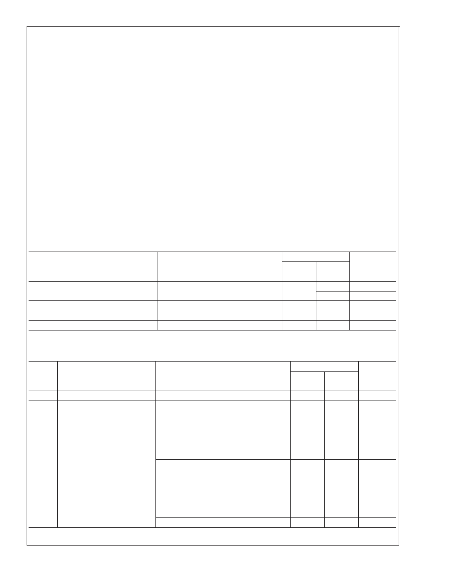
Absolute Maximum Ratings (Note 3)
If Military/Aerospace specified devices are required,
please contact the National Semiconductor Sales Office/
Distributors for availability and specifications.
Supply Voltage
6.0V
Storage Temperature
65C to +150C
Input Voltage
0.3V to V
DD +0.3V
Power Dissipation (Note 4)
Internally limited
ESD Susceptibility (Note 5)
All pins except Pin 3 (MT, MTE), Pin 2 (LQ)
2000V
Pin 3 (MT, MTE), Pin 2 (LQ)
8000V
ESD Susceptibility (Note 6)
200V
Junction Temperature
150C
Solder Information
Small Outline Package
Vapor Phase (60 sec.)
215C
Infrared (15 sec.)
220C
See AN-450 “Surface Mounting and their Effects on
Product Reliablilty” for other methods of soldering
surface mount devices.
Thermal Resistance
θ
JC (typ) — MTC20
20C/W
θ
JA (typ) — MTC20
80C/W
θ
JC (typ) — MXA20A
2C/W
θ
JA (typ) — MXA20A
41C/W (Note 7)
θ
JA (typ) — MXA20A
51C/W (Note 8)
θ
JA (typ) — MXA20A
90C/W (Note 9)
θ
JC (typ) — LQA24A
3.0C/W
θ
JA (typ) — LQA24A
42C/W (Note 10)
Operating Ratings
Temperature Range
T
MIN
≤ T
A
≤ T
MAX
40C
≤ T
A
≤ 85C
Supply Voltage
2.0V
≤ V
DD
≤ 5.5V
Electrical Characteristics for Entire IC (Notes 3, 11)
The following specifications apply for V
DD= 5V unless otherwise noted. Limits apply for TA= 25C.
Symbol
Parameter
Conditions
LM4867
Units
(Limits)
Typical
Limit
V
DD
Supply Voltage
2
V (min)
5.5
V (max)
I
DD
Quiescent Power Supply Current
V
7.5
15
mA (max)
V
3.0
6
mA (max)
I
SD
Shutdown Current
V
DD applied to the SHUTDOWN pin
0.7
2
A (max)
Electrical Characteristics for Bridged-Mode Operation (Notes 3, 11)
The following specifications apply for V
DD= 5V unless otherwise specified. Limits apply for TA= 25C.
Symbol
Parameter
Conditions
LM4867
Units
(Limits)
Typical
Limit
V
OS
Output Offset Voltage
V
IN = 0V
5
50
mV (max)
P
O
Output Power (Note 15)
THD = 1%, f = 1kHz (Note 16)
LM4867MTE, R
L =3
2.2
W
LM4867LQ, R
L =3
2.4
W
LM4867MTE, R
L =4
1.9
W
LM4867LQ, R
L =4
2.1
W
LM4867, R
L =8
1.1
1.0
W (min)
THD+N = 10%, f = 1kHz (Note 16)
LM4867MTE, R
L =3
3.0
W
LM4867LQ, R
L =3
3.0
W
LM4867MTE, R
L =4
2.6
W
LM4867LQ, R
L =4
2.6
W
LM4867, R
L =8
1.5
W
THD+N = 1%,f=1 kHz, R
L =32
0.34
W
LM4867
www.national.com
3
发布紧急采购,3分钟左右您将得到回复。
相关PDF资料
LM4867LQX/NOPB
3 W, 2 CHANNEL, AUDIO AMPLIFIER, PQCC24
LM4882MM/NOPB
0.48 W, 1 CHANNEL, AUDIO AMPLIFIER, PDSO8
LM4882M/NOPB
0.48 W, 1 CHANNEL, AUDIO AMPLIFIER, PDSO8
LM556ICN
DUAL PULSE; RECTANGULAR, TIMER, PDIP14
LM5756
3.5 A SWITCHING REGULATOR, 100 kHz SWITCHING FREQ-MAX, ZFM5
LM7001JM
PLL FREQUENCY SYNTHESIZER, 130 MHz, PDSO20
LM7001M
PLL FREQUENCY SYNTHESIZER, 130 MHz, PDSO20
LM7006
PLL FREQUENCY SYNTHESIZER, 400 MHz, PDIP20
相关代理商/技术参数
LM4867MT
制造商:NSC 制造商全称:National Semiconductor 功能描述:Output-Transient-Free Dual 2.1W Audio Amplifier Plus No Coupling Capacitor Stereo Headphone Function
LM4867MT NOPB
制造商:Texas Instruments 功能描述:Audio Amp Headphone/Speaker 2-CH Stereo 1.5W Class-AB 20-Pin TSSOP Rail
LM4867MT/NOPB
功能描述:IC AMP AUDIO PWR 3W AB 20TSSOP RoHS:是 类别:集成电路 (IC) >> 线性 - 音頻放大器 系列:Boomer® 产品培训模块:Lead (SnPb) Finish for COTS
Obsolescence Mitigation Program 标准包装:2,500 系列:DirectDrive® 类型:H 类 输出类型:耳机,2-通道(立体声) 在某负载时最大输出功率 x 通道数量:35mW x 2 @ 16 欧姆 电源电压:1.62 V ~ 1.98 V 特点:I²C,麦克风,静音,短路保护,音量控制 安装类型:表面贴装 供应商设备封装:25-WLP(2.09x2.09) 封装/外壳:25-WFBGA,WLCSP 包装:带卷 (TR)
LM4867MTE
制造商:Texas Instruments 功能描述:Audio Amp Headphone/Speaker 2-CH Stereo 3W Class-AB 20-Pin TSSOP EP Rail
LM4867MTE/NOPB
功能描述:IC AMP AUDIO PWR 3W AB 20TSSOP RoHS:是 类别:集成电路 (IC) >> 线性 - 音頻放大器 系列:Boomer® 产品培训模块:Lead (SnPb) Finish for COTS
Obsolescence Mitigation Program 标准包装:2,500 系列:DirectDrive® 类型:H 类 输出类型:耳机,2-通道(立体声) 在某负载时最大输出功率 x 通道数量:35mW x 2 @ 16 欧姆 电源电压:1.62 V ~ 1.98 V 特点:I²C,麦克风,静音,短路保护,音量控制 安装类型:表面贴装 供应商设备封装:25-WLP(2.09x2.09) 封装/外壳:25-WFBGA,WLCSP 包装:带卷 (TR)
LM4867MTEX
制造商:National Semiconductor Corporation 功能描述:Audio Amplifier Circuit, Dual, 20 Pin, Plastic, TSSOP
LM4867MTEX/NOPB
功能描述:IC AMP AUDIO PWR 3W AB 20TSSOP RoHS:是 类别:集成电路 (IC) >> 线性 - 音頻放大器 系列:Boomer® 产品培训模块:Lead (SnPb) Finish for COTS
Obsolescence Mitigation Program 标准包装:2,500 系列:DirectDrive® 类型:H 类 输出类型:耳机,2-通道(立体声) 在某负载时最大输出功率 x 通道数量:35mW x 2 @ 16 欧姆 电源电压:1.62 V ~ 1.98 V 特点:I²C,麦克风,静音,短路保护,音量控制 安装类型:表面贴装 供应商设备封装:25-WLP(2.09x2.09) 封装/外壳:25-WFBGA,WLCSP 包装:带卷 (TR)
LM4867MTX/NOPB
功能描述:IC AMP AUDIO PWR 3W AB 20TSSOP RoHS:是 类别:集成电路 (IC) >> 线性 - 音頻放大器 系列:Boomer® 产品培训模块:Lead (SnPb) Finish for COTS
Obsolescence Mitigation Program 标准包装:2,500 系列:DirectDrive® 类型:H 类 输出类型:耳机,2-通道(立体声) 在某负载时最大输出功率 x 通道数量:35mW x 2 @ 16 欧姆 电源电压:1.62 V ~ 1.98 V 特点:I²C,麦克风,静音,短路保护,音量控制 安装类型:表面贴装 供应商设备封装:25-WLP(2.09x2.09) 封装/外壳:25-WFBGA,WLCSP 包装:带卷 (TR)